- Advanced Interconnect Technologies
- 2.5 & 3D Heterogeneous Integration
- System in Package (SiP)
- Wafer Bumping & WLP
- Multi-Chip Modules (MCMs)
- Novel Microfabrication & MEMS
- Design, Packaging & Assembly
- Assembly Services
- Final Test
- Chip on Board (CoB)
- Plastic Packaging (BGA/CSP/QFN)
- Hermetic Packaging
- MIL-STD-1553 Data Bus Couplers & Accessories
- Micro In-Line Couplers
- Tab Mounted In-Line Couplers
- Through Hole Mounted In-Line Couplers
- Box Couplers
- Custom Design Couplers
- Data Bus Coupling Transformers
- Data Bus Relays
- Data Bus Harnesses
- Bus and Stub Terminators
- Wide Bandwidth RF & Video Transformers
- Antenna Couplers
- Video Isolation Transformers
- RF Wideband Transformers
- RF Wideband Transformers & Impedance Adapters
Advanced Interconnect Technologies
System in Package (SiP)
Next level integration with our reliable, highly integrated assembly alternative, utilizing available active semiconductor die and discretes
More infoWafer Bumping & WLP
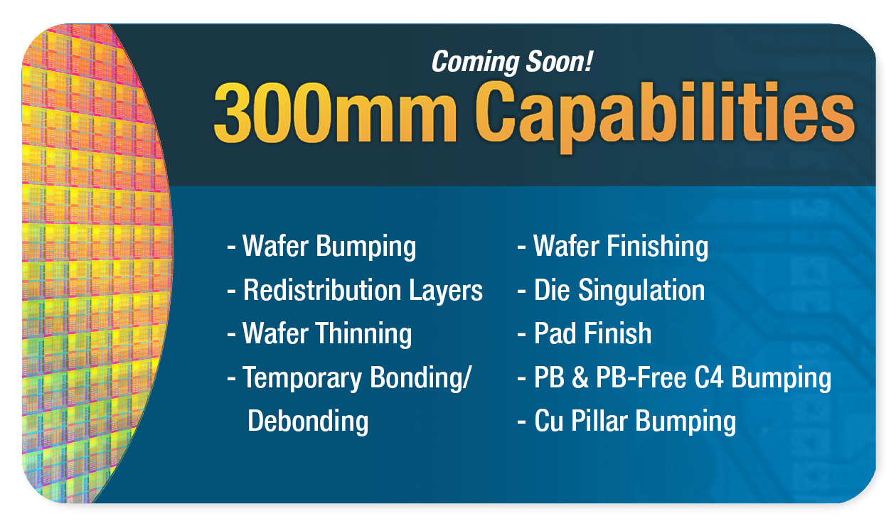
Supporting wafer sizes up to 200mm with established and proven WLP processes and flexibility to tailor unique solutions
More infoMulti-Chip Modules (MCMs)
Flip chip assembly, precision die placement, heterogeneous integration, plasma assisted dry soldering (PADS) process
More infoNovel Microfabrication & MEMS
Wafer-level vacuum packaging, monolithic device integration, 3D microstructures for vacuum microelectronics
More infoDesign, Packaging & Assembly
Assembly Services
Comprehensive array of in-house assembly capabilities that spans both the United States and Europe
More infoFinal Test
STS performs the final quality assurance test to identify latent defects that could cause failures in the early operation
More infoChip on Board (CoB)
Low cost integration facilitating single or multiple active & discrete components with a reliable assembly alternative
More infoPlastic Packaging (BGA/CSP/QFN)
Chip scale packages offer near-die size footprints and reduce package thickness and weight
More infoHermetic Packaging
Ceramic, metal can, two/four-sided LCC, gull wing, QFP, PGA, flat pack, formed-leaded flat pack
More info


