

- Die & Wafer
- +Supplier Line Card
- Alliance Memory
- Analog Devices
- Apogee Semiconductor
- Analog Power
- Avalanche Technology
- Central Semiconductor
- Diodes Incorporated
- Cypress
- Everspin Technologies
- Interfet
- International Rectifier
- ISOCOM Limited
- ISSI
- Knowles
- Linear Integrated Systems
- MACOM Technology
- Microchip
- Micron Technology
- NXP Semiconductors
- On Semi
- Renesas
- Samsung Semiconductors
- SemiQ Inc.
- Semicoa
- Texas Instruments
- +Supplier Line Card
- Transys
- Vishay
- VPT Components
- Advanced Interconnect Technologies
- 2.5 & 3D Heterogeneous Integration
- System in Package (SiP)
- Multi-Chip Modules (MCMs)
- Wafer Bumping & WLP
- Design, Packaging & Assembly
- Assembly Services
- Chip on Board (CoB)
- Plastic Packaging (BGA/CSP/QFN)
- Hermetic Packaging
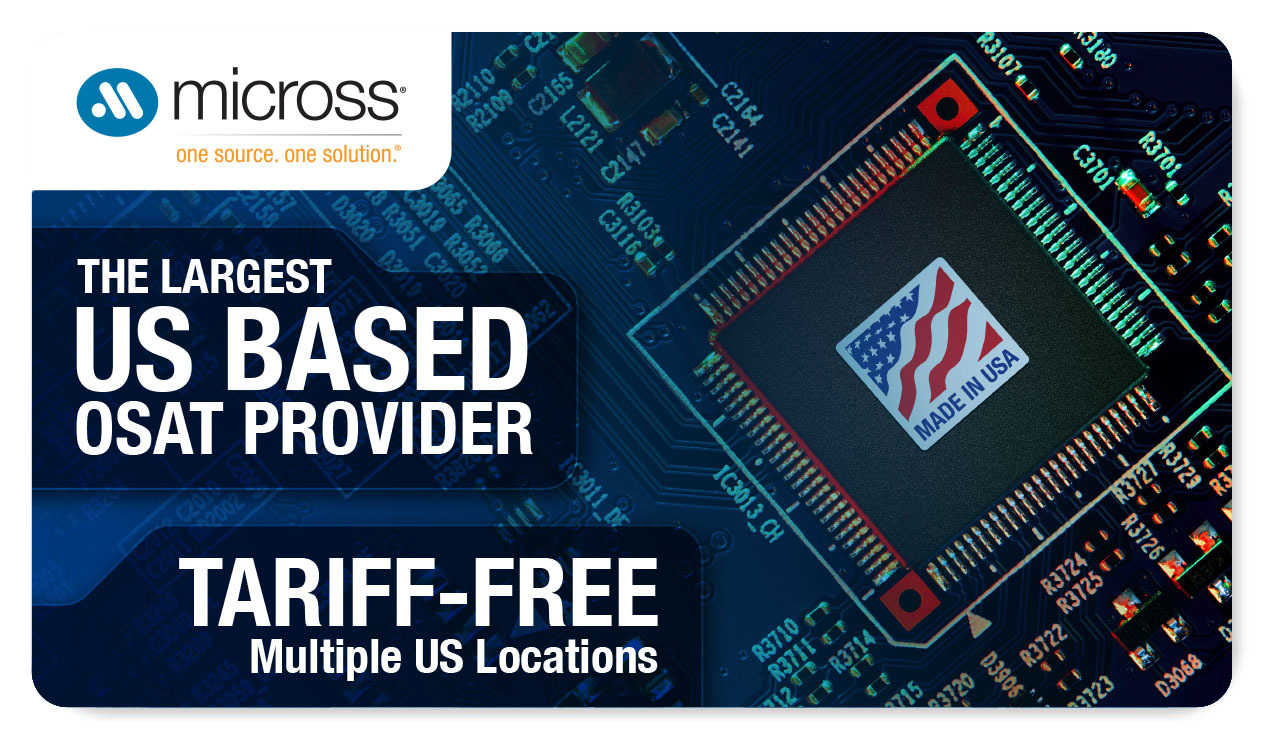
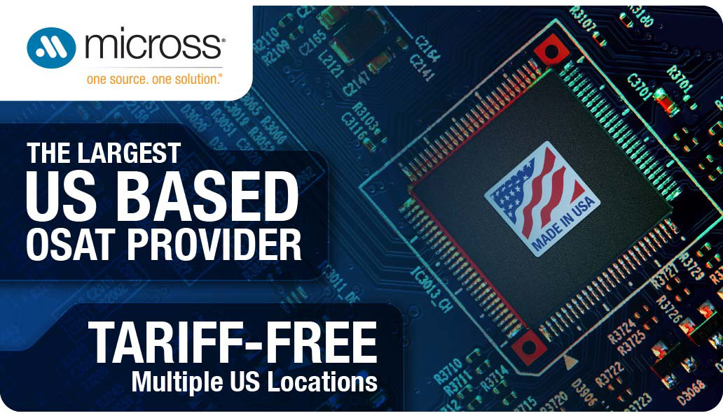
In a world where over 95% of semiconductor assembly and test services are outsourced beyond U.S. borders, costs are vulnerable to spikes. But here's a game-changer: Micross stands as the largest OSAT manufacturer right here in the United States.
For over 45 years, Micross has been the backbone of the aerospace, defense, space, medical, automotive, and communications sectors, delivering the most comprehensive suite of microelectronic products and services globally. As a DMEA DoD Trusted Source OSAT provider, Micross empowers U.S.-based electronics manufacturers to sidestep risks, bypass delays, and cut additional costs—all while enjoying Tariff-Free procurement!
Die Prep
Wafer Thinning & Dicing
Wafers thinned down to 100µm, dicing of wafer sizes up to and including 12” (300mm)
More infoDie Plating / Customized Output
Automated, virtually contactless handling of singulated die, multiple bin/grade die picking
More infoVisual Inspection
Acceptable Quality Level (AQL), MIL-STD, inspection via AOI equipment available, up-to-date automatic inspection equipment
More infoLot Acceptance Testing
Conversion between industry formats, inking using any electronic wafer map
More infoAssembly
2.5/3D Heterogeneous Packaging
Offering access through joint development projects, prototyping services and small volume production
More infoHermetic & Plastic Packaging
More infoWafer Bumping
Supporting wafer sizes up to 200mm with established and proven WLP processes and flexibility to tailor unique solutions
More infoComponent Modification
Utilize the latest COTS components, chip designs, and technology in your hi-rel application.
More infoTest
Up-Screening
Utilize the latest COTS technologies in space. Complete turnkey solutions for PEM-Qualification
More infoElectrical Testing
Leading capabilities and expertise for ICs used in analog, digital, mixed and RF signal processing applications
More infoEnvironmental Testing
Complete environmental testing solutions including HTOL/LTOL, HAST, HTSL, THB and many others
More infoReliability Testing
Reliability plans designed for suitability of use, interaction in subsystems, field use, & storage
More infoCounterfeit Mitigation
Independent third-party counterfeit lab. AS6081 & AS7161 counterfeit testing services
More infoComponent Inspection
Acoustic Microscopy, X-Ray, X-Ray Fluorescencem and IPC-A-610 inspection services
More infoWafer Probe
In-house expertise to design test programs and perform the wafer testing and sorting
More info