- Die & Wafer
- +Supplier Line Card
- Alliance Memory
- Analog Devices
- Apogee Semiconductor
- Analog Power
- Avalanche Technology
- Central Semiconductor
- Diodes Incorporated
- Cypress
- Everspin Technologies
- Interfet
- International Rectifier
- ISOCOM Limited
- ISSI
- Knowles
- Linear Integrated Systems
- MACOM Technology
- Microchip
- Micron Technology
- NXP Semiconductors
- On Semi
- Renesas
- Samsung Semiconductors
- SemiQ Inc.
- Semicoa
- Texas Instruments
- +Supplier Line Card
- Transys
- Vishay
- VPT Components
- Advanced Interconnect Technologies
- 2.5 & 3D Heterogeneous Integration
- System in Package (SiP)
- Multi-Chip Modules (MCMs)
- Wafer Bumping & WLP
- Design, Packaging & Assembly
- Assembly Services
- Chip on Board (CoB)
- Plastic Packaging (BGA/CSP/QFN)
- Hermetic Packaging
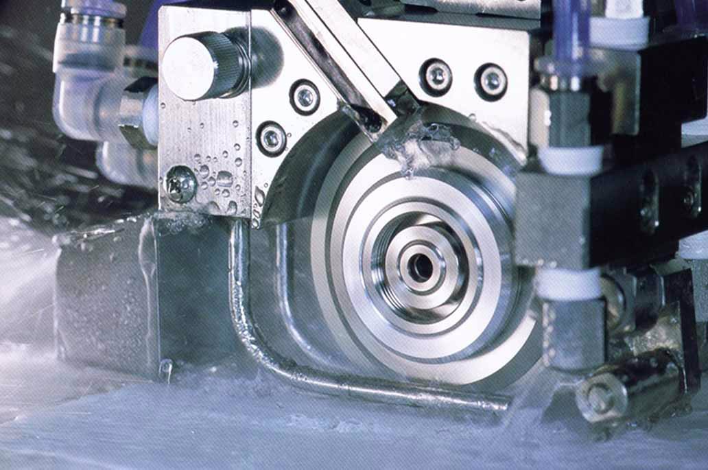
Wafer dicing is an essential requirement of anyone using die in their applications. Wafers can vary in size and materials and have as few as a hundred die or well over a hundred thousand on them. There are three main types of dicing processes today. Mechanical sawing uses a saw blade to cut through the wafers. The scribe and brake process, and stealth dicing or laser cutting. It's important to know what type of material your wafer is. Know what the size of the wafer is so that we know which process can best support your needs. Users of gas wafers, for example, are more and more leaning towards laser dicing for its speed and consistent cutting quality as they tend to be more fragile than your standard silicon wafers.
Our Capabilities:
- Wafers Thinned Down to 100µm
- Employing dry polishing to remove substrate damage
- Wafer Sizes Up to and Including 12" (300mm)
- ±1µm Tolerance for Dicing/Sawing
- Custom Dicing Plans, Multi-Project Wafers
- Can Process Most Non-Silicon Materials


